Technologies
at Scale
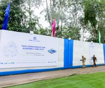
Our fast-upcoming greenfield facility in Jagiroad, Assam, is slated to begin operations in 2025. Our investment of over $3 billion will attract a global ecosystem to India, enhancing supply chain resilience.
Our portfolio of traditional and advanced packaging technologies, delivered at scale, provides competitive advantages to our global customer base.
Our Locations

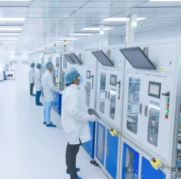
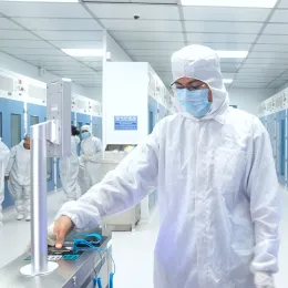
First Commercial Facility, Vemgal, Karnataka
- State-of-the-art facilities
- World class equipment
- ISO 9001 certified
- Operational since Dec 2023
First Commercial Facility, Vemgal, Karnataka
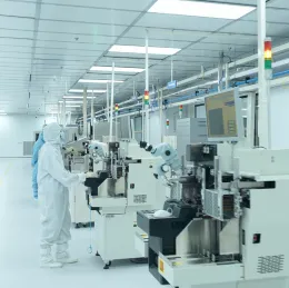
HVM Greenfield Facility, Jagiroad, Assam
HVM Greenfield Facility, Jagiroad, Assam
- USD 3Bn+ investment
- 600-acre campus near Guwahati
- 100% renewable energy
- Ready for high volume manufacturing by mid 2025

1000+
years of combined expertise
600-acre
Large campus

$3+ Bn
investment
15+ Bn
chips per year capacity
Join Us
AI-enabled
factories
3
packaging technology & expanding

100% renewable power from day 1
2 Mn ft 2
operational area, 50% cleanroom space

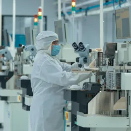
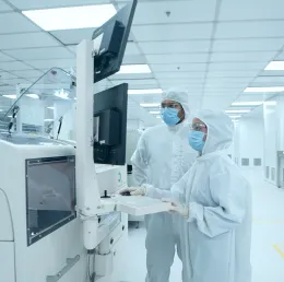
Our Capability
Our proven expertise enables us to address the evolving needs of the semiconductor market, providing a complete range of solutions from packaging to testing and failure analysis.
- Package Design
- Wafer/Die Preparation
- Interconnection
- Finishing
- Testing
- Failure Analysis & Reliability

Package Design
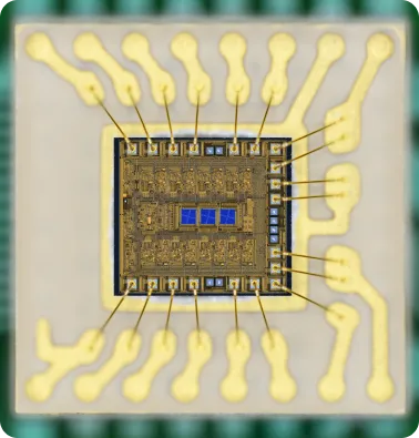
IC Package Design is a vital step in semiconductor manufacturing that determines how an integrated circuit (IC) is interconnected, encapsulated, and integrated with external systems. The design ensures the IC functions optimally by addressing key factors such as electrical performance, thermal management, mechanical protection, and long-term reliability.

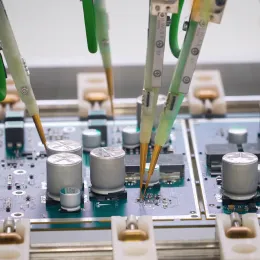
Wafer/Die Preparation
Wafer/Die Preparation transforms a silicon wafer embedded with integrated circuits (ICs) into separate functional chips. This process includes essential steps like thinning the wafer, singulating the wafer into individual dies, and pick-and-place.

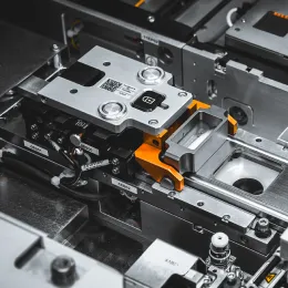
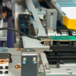
Interconnection
Interconnection in IC packaging establishes electrical connections between the IC die and external systems, impacting performance, signal integrity, reliability, and functionality. The choice of technique-such as wire bonding, flip-chip, or TSVs depends on the IC's performance needs, package type, space and cost constraints.

Finishing
Finishing involves molding or encapsulating the die for protection, followed by deflashing, which meticulously removes any surplus molding compound. Then, laser marking provides permanent identification and traceability. Finally, singulation separates individual units from the lead frame or substrate, preparing the IC for final testing and shipment.

Testing
Testing in IC Packaging is an essential step that ensures the integrated circuit (IC) functions as intended, remains reliable over its lifespan, and meets all required performance specifications after packaging. This phase is essential for verifying the IC's functionality, durability, and quality before it is integrated into final products, ensuring that it meets the standards for real-world application.

Failure Analysis & Reliability
Failure Analysis is a systematic approach used to investigate and identify the root causes of IC failures, focusing on packaging and interconnect issues. It helps improve designs and prevent future failures and reliability evaluates how ICs perform under operational stresses like thermal cycles, mechanical shocks, vibrations, and humidity. This testing ensures the IC will maintain performance and durability in real-world conditions.
Packaging Technology
Our proven expertise enables us to address the evolving needs of the semiconductor market, providing a complete range of solutions from packaging to testing and failure analysis.
Wire Bond
Wire Bond is a key interconnection method that establishes electrical links between the IC's bond pads and external leads or pads of the package using fine wires made of Gold, Aluminum, or Copper. It ensures reliable power and signal transfer between the die and the package.
Integrated System Packaging (ISP)
Integrated System Packaging (ISP) is a transformative technology that enables the integration of diverse system components such as microprocessors, memory chips, sensors, power management circuits, and passive components into a single, compact, high-performance package. It delivers enhanced functionality while minimizing the overall form factor.
Flip Chip
Flip Chip is a high-density interconnection technique where solder bumps are precisely deposited on the IC's bond pads reducing signal path length, minimizing parasitics, and enhancing thermal performance.
Wafer-Level Packaging (WLP) is a packaging method in which the entire wafer undergoes packaging processes such as bumping and encapsulation before being diced into individual chips.
Market Segments
We are focusing on a diverse array of market segments with our packaging technologies.

Artificial Intelligence

Mobile

Storage
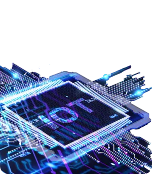
Internet of Things

Automotive

Radio Frequency
Certifications

Certification Roadmap
Partnerships
We have tied up with premier institutes for further innovations and technical collaborations.

Indian Institute of Management, Mumbai
Executive MBA in Manufacturing Management

Sastra University
MTech. in VLSI